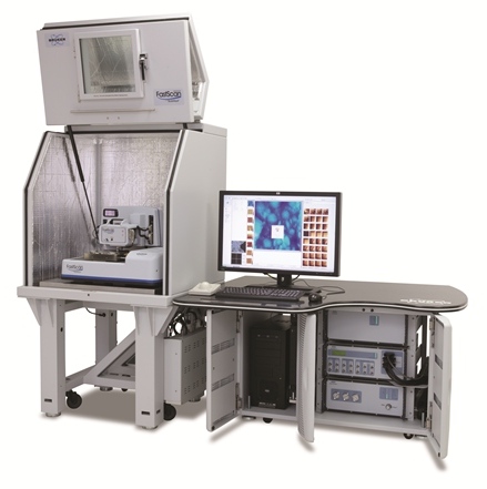
The Dimension FastScan is a high speed multiple mode scanning probe microscope for morphological, phase, electrochemical and electrical characterization of solids, polymers and biological material on the nano-scale. It is the fastest SPM on the market, allowing the monitoring of dynamic processes on a time scale of seconds. The ultimate height resolution is less than a nanometer.
It features exceptional force control and high scan rates (as little as 1 sec per image frame).
The FastScan offers over 30 modes of operation: Apart from standard modes such as Tapping, Contact, Lift (including Magnetic and Electric Force modes), and Phase Imaging, the FastScan incorporates:
-
ScanAsyst, allowing automated configuration of scan parameters enabling inexperienced users to obtain high quality images without advanced training.
-
Nanomechanical mapping provides quantitative analysis of e.g. elastic modulus, deformation, adhesion.
-
Lateral Force mode, which maps differences in frictional forces across the surface.
-
The unique PeakForce tapping mode decreases sample and tip wear and enhances other SPM modes.
-
Torsional Resonance mode provides information on in-plane anisotropy and dynamic friction.
-
Surface Potential mode (Kelvin Force probe microscopy) allows quantification of the surface Fermi-level of material.
-
PeakForce Tunneling AFM mode (similar to conductive AFM, but with higher sensitivity) allows mapping of the conductivity of low to medium conducting and semiconducting materials (analysis of soft materials and loosely bound particles like nanorods is also possible).
-
Scanning Capacitance mode, which maps the majority carrier concentration in moderately to highly doped semiconductors.
-
Electrochemical AFM allows the nano-scale mapping of electrode surfaces.
-
Scanning spreading resistance microscopy, AFM, which allows mapping of carrier concentrations over a broad range (1015 to 1020 carriers/cc), and can resolve features as small as 10nm on sharp doping transitions. Can be used to examine cross-sections through submicron gate length transistors, providing contrast of doping structures, such as source/drain/well implants, doped polysilicon, and LDDs (lightly-doped drain). Can also be used to image variations in conductivity for various semiconductor and non-semiconductor materials.
-
STM mode provides information on the atomic scale for studies of surface contamination, surface reconstruction and atomic step arrangements.